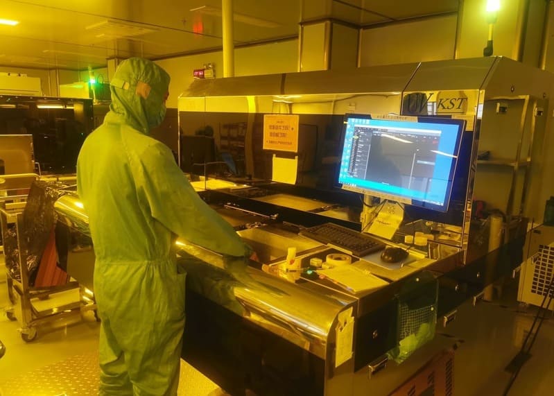
KST's direct imaging (DI) solutions for patterning enable PCB manufacturers to achieve the best imaging results with the highest throughput.
Our DI systems help decrease overall cost of ownership while maintaining optimal quality at high speeds. Powered by MultiWave UV LED technology, and based on KST's own LED light source and Optical camera technology, our solutions achieve enhanced depth-of-focus for superior results on panel topography changes, as well as best line uniformity.

|
No. |
Item |
KST-DI2428-6XLB |
KST-DI2428-12XLB |
|
1 |
PCB size(Max) |
24.5" * 28.5 " |
24.5 " * 28.5 " |
|
2 |
PCB size (Min) |
25 " * 21 "【Clampable】 16 " * 16 "【Customizable Clamp Structure】 12 " * 12 "【Non Clampable】 |
25 " * 21 "【Clampable】 16 " * 16 "【Customizable Clamp Structure】 12 " * 12 "【Non Clampable】 |
|
3 |
PCB Thickness |
0.08 – 4.0mm |
|
|
4 |
Clamp Structure |
Yes |
|
|
5 |
Line Resolution |
50um/50um |
|
|
6 |
Light Source depth of field |
±300um |
|
|
7 |
Alignment Accuracy |
±12um |
|
|
8 |
Processing Speed |
24.5" *28.5" PCB Dry film 2.5 – 3 PNL /min High sensitive ink,Dry film 3.5 PNL/min; |
|
|
9 |
Sensitive material |
Dry film, Wet film |
|
|
10 |
Laser/DMD No. |
6(Total 6) |
12(Total 12) |
|
11 |
Uniformity |
≥90% |
|