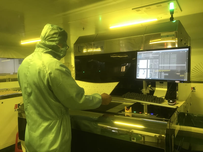
Direct Imaging for PCB Solder Mask
KST's leading direct imaging (DI) solutions for solder mask (SM) deliver high accuracy, high quality imaging and high throughput for any solder mask design, from the simplest to the most complex. These high-capacity, field-proven solutions for mass production leverage KST unique proprietary technologies to ensure consistently high imaging quality with a low total cost of ownership.

|
No. |
Item |
KST-DI2428-6FEB |
KST-DI2428-12FEB |
|
1 |
PCB size(Max) |
24.5"* 28.5" |
24.5 inch * 28.5 inch |
|
2 |
PCB size(Min) |
24.5" * 21 "【Clampable】 12 " * 12 "【Non Clampable】 |
24.5 inch * 21 inch【Clampable】 12 inch * 12 inch【Non Clampable】 |
|
3 |
PCB Thickness |
0.15 - 4.0mm |
|
|
4 |
Clamp Structure |
Yes |
|
|
5 |
Bridge and Opening Size |
Green ink Bridge :50um / Solder Mask Opening 75um |
|
|
6 |
Light Source depth of field |
±300um |
|
|
7 |
Alignment Accuracy |
±15um |
|
|
8 |
Processing Speed |
24.5"*28.5" PCB TAIYO INK 1 – 1.5 side /min High sensitive ink 2 side/min; |
24.5inch*28.5inch PCB TAIYO INK 2 – 2.5 side /min High sensitive ink 3~3.5 side/min; |
|
9 |
Sensitive material |
TAIYO INK; Special ink for DI |
|